Improving the lifetime of state-of-the-art EUV lithography optics through atomistic material calculations

In a joint EU project, Fraunhofer IWM is working in a consortium led by ASML to achieve the ambitious goals set by the EU for expanding local computer chip manufacturing in Europe. The aim of the project "14 AMI" is to reduce the resolution of EUV (extreme ultra violet, EUV) lithography systems to 14 angstroms, while improving the throughput of the complex and expensive EUV systems through increased lifetime. Our consortium is supported by the Chips Joined Undertaking “Chips JU” (formerly known as "KDT JU") and its members, including the top-up funding by the German Federal Ministry of Education and Research (BMBF).
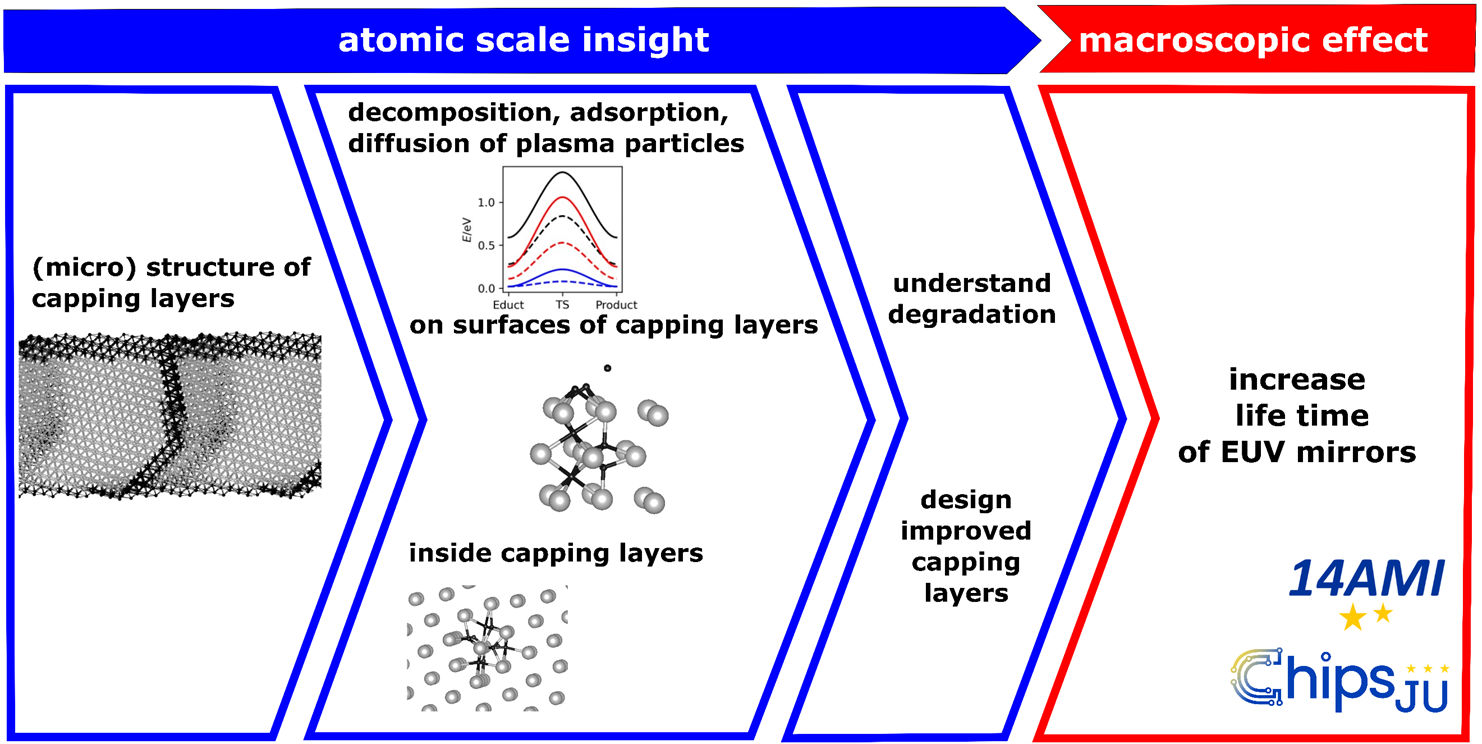
At Fraunhofer IWM, we mainly work on elucidating phenomenologically observed indications of degradation of mirror systems through computer calculations on an atomic scale. This allows us to understand the observed material failure and derive steps to prevent it. Technically, this means understanding the (micro)structure of the protective layers of the mirror systems and defining suitable model systems on an atomic scale. For these model systems, the relevant processes of interaction between plasma particles and the protective layers are calculated, i.e., the chemical and physical processes of decomposition, absorption, and diffusion. We describe these quantitatively using calculations within the framework of density-functional theory. Based on the insights gained, steps can be derived to improve the protective layers that have been used so far. The evaluation of the (modified) protective layers is then carried out directly on the atomic scale or by transferring the quantitative results into simulations on a higher scale.
Back to Assessment of Materials and Lifetime Concepts Highlights
 Fraunhofer Institute for Mechanics of Materials IWM